“It is chemically, mechanically and thermally robust and can be patterned and seamlessly connected to semimetallic epigraphene using conventional semiconductor fabrication techniques.”
Sounds promising.
Can someone explain the implications of the bandgap and room temperature mobility values for future chip designs?
My possibly wrong, not researched, and half remembered from college first impressions are: the band gap is lower than Silicon, so it might not be appropriate in room temperature applications/very small gate sizes due to dark current. But the mobility is very high, meaning lower voltage gates might be possible, or higher switching speed/lower latency gates.
Half the band gap of silicon, 10 times the mobility, at room temperature… sounds like it would be able to switch up to 20 times faster in the same conditions.
I can’t read the full paper, but what I’d wonder is how those values change with temperature:
0.6eV at 300K is similar to Germanium, which has slightly lower mobility but has been successfully used in semiconductors. If graphene has a better dimensional stability (as in, doesn’t grow random dendrites over time), then it could be a decent improvement.
As far as I understand (I haven’t had much experience with high frequencies), it depends on the amount of energy you are willing to push.
Smaller band gap and higher mobility, means less energy needed to switch, but also higher sensitivity to random noise. If you want to “transmit” a high frequency signal, you want a larger signal eye, which for a single signal, you can do by increasing the energy. However, if you want a few billion transistors, each one with “its own signal”, then you want to reduce energy usage first, think about ways to shield them from the noise later.
For reference, a modern CPU running at 0.6V with a 50W TDP, means it potentially could be pulling up to 80A internally. Reducing that by half, would directly allow 4 times more simultaneously active transistors at the same TDP. Having them switch 20 times faster, if you managed to deal with the noise, it would pave the way to 80 times faster multiprocessors for a similar power budget.
The good news is, if they use less energy, then they also emit less noise, which decays with the square of the distance. So half the emitted noise, even with twice the noise susceptibility, could let you pack them twice as close, meaning 4x as many per area, or 8x as many per volume.


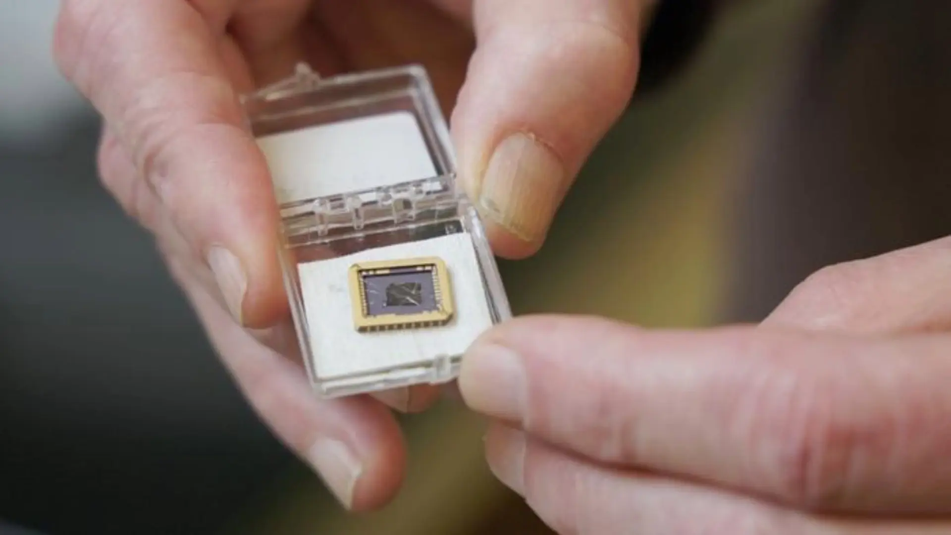
“It is chemically, mechanically and thermally robust and can be patterned and seamlessly connected to semimetallic epigraphene using conventional semiconductor fabrication techniques.”
Sounds promising.
Can someone explain the implications of the bandgap and room temperature mobility values for future chip designs?
My possibly wrong, not researched, and half remembered from college first impressions are: the band gap is lower than Silicon, so it might not be appropriate in room temperature applications/very small gate sizes due to dark current. But the mobility is very high, meaning lower voltage gates might be possible, or higher switching speed/lower latency gates.
Half the band gap of silicon, 10 times the mobility, at room temperature… sounds like it would be able to switch up to 20 times faster in the same conditions.
I can’t read the full paper, but what I’d wonder is how those values change with temperature:
0.6eV at 300K is similar to Germanium, which has slightly lower mobility but has been successfully used in semiconductors. If graphene has a better dimensional stability (as in, doesn’t grow random dendrites over time), then it could be a decent improvement.
if anything SiC support is as stiff as they come
wait, last time i’ve checked if you want fast switching, faster than silicon can get you, you use GaN, and it has 3.4eV band gap. how does it work?
As far as I understand (I haven’t had much experience with high frequencies), it depends on the amount of energy you are willing to push.
Smaller band gap and higher mobility, means less energy needed to switch, but also higher sensitivity to random noise. If you want to “transmit” a high frequency signal, you want a larger signal eye, which for a single signal, you can do by increasing the energy. However, if you want a few billion transistors, each one with “its own signal”, then you want to reduce energy usage first, think about ways to shield them from the noise later.
For reference, a modern CPU running at 0.6V with a 50W TDP, means it potentially could be pulling up to 80A internally. Reducing that by half, would directly allow 4 times more simultaneously active transistors at the same TDP. Having them switch 20 times faster, if you managed to deal with the noise, it would pave the way to 80 times faster multiprocessors for a similar power budget.
The good news is, if they use less energy, then they also emit less noise, which decays with the square of the distance. So half the emitted noise, even with twice the noise susceptibility, could let you pack them twice as close, meaning 4x as many per area, or 8x as many per volume.